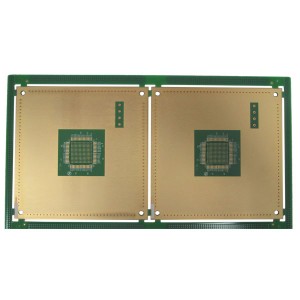
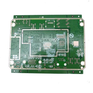
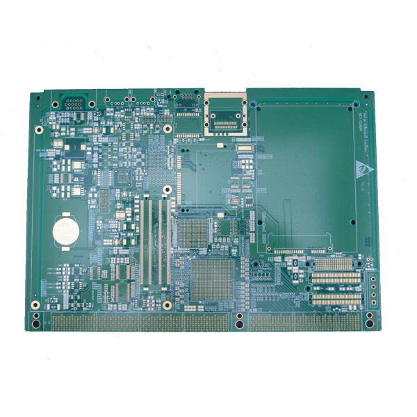
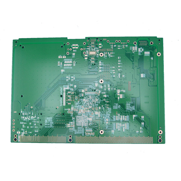
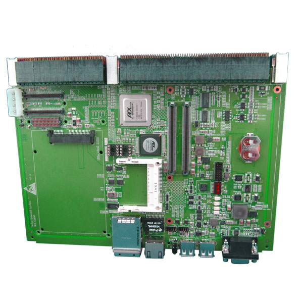
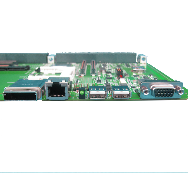
HDI Circuit board for embedded system
Product Details
| Layers | 10 layers |
| Board thickness | 1.6MM |
| Material | IT-180A Tg170 |
| Copper thickness | 1 OZ(35um) |
| Surface Finish | (ENIG) Immersion gold |
| Min Hole(mm) | 0.20mm Mechanical blind via |
| Via technology | Via plugged with resin |
| Min Line Width(mm) | 0.10mm (4 mil) |
| Min Line Space(mm) | 0.10mm (4 mil) |
| Solder Mask | Green |
| Legend Color | White |
| Impedance | Single Impedance & Differential Impedance |
| Packing | Anti-static bag |
| E-test | Flying probe or Fixture |
| Acceptance standard | IPC-A-600H Class 2 |
| Application | Embedded System |
1. Introduction
HDI stands for High Density Interconnector. A circuit board which has a higher wiring density per unit area as opposed to conventional board is called as HDI PCB. HDI PCBs have finer spaces and lines, minor vias and capture pads and higher connection pad density. It is helpful in enhancing electrical performance and reduction in weight and size of the equipment. HDI PCB is the better option for high-layer count and costly laminated boards.
Key HDI Benefits
As consumer demands change, so must technology. By using HDI technology, designers now have the option to place more components on both sides of the raw PCB. Multiple via processes, including via in pad and blind via technology, allow designers more PCB real estate to place components that are smaller even closer together. Decreased component size and pitch allow for more I/O in smaller geometries. This means faster transmission of signals and a significant reduction in signal loss and crossing delays.
Technologies in HDI PCB
- Blind Via: Contacting of an outer layer ending on an inner layer
- Buried Via: Through-hole in the core layers
- Microvia: Blind Via (coll. also via) with a diameter ≤ 0.15mm
- SBU (Sequential Build-Up): Sequential layer buildup with at least two press operations on multilayer PCBs
- SSBU (Semi Sequential Build-Up): Pressing of testable substructures in SBU technology
Via in Pad
Inspiration from surface mount technologies from the late 1980's has pushed the limits with BGA's, COB and CSP into smaller square surface inches. The via in pad process allows for vias to be placed within the surface of the flat lands. The via is plated and filled with either conductive or non-conductive epoxy then capped and plated over, making it virtually invisible.
Sounds simple but there is an average of eight additional steps to complete this unique process. Specialty equipment and trained technicians follow the process closely to achieve the perfect hidden via.
Via Fill Types
There are many different types of via fill material: non conductive epoxy, conductive epoxy, copper filled, silver filled and electrochemical plating. These all result in a via buried within a flat land that will completely solders as normal lands. Vias and microvias are drilled, blind or buried, filled then plated and hidden beneath SMT lands. Processing vias of this type requires special equipment and is time consuming. The multiple drill cycles and controlled depth drilling adds to process time.
Laser Drill Technology
Drilling the smallest of micro-vias allows for more technology on the board's surface. Using a beam of light 20 microns (1 Mil) in diameter, this high influence beam can cut through metal and glass creating the tiny via hole. New products exist such as uniform glass materials that are a low loss laminate and low dielectric constant. These materials have higher heat resistance for lead free assembly and allow for the smaller holes to be used.
Lamination & Materials For HDI Boards
Advanced multilayer technology allows for designers to sequentially add additional pairs of layers to form a multilayer PCB. The use of a laser drill to produce holes in the internal layers allows for plating, imaging and etching prior to pressing. This added process is known as sequential build up. SBU fabrication uses solid filled vias allowing for better thermal management, a stronger inter connect and increasing the board's reliability.
Resin coated copper was developed specifically to aide with poor hole quality, longer drill times and to allow for thinner PCBs. RCC has an ultra-low profile and ultra-thin copper foil that is anchored with minuscule nodules to the surface. This material is chemically treated and primed for the thinnest and finest line and spacing technology.
The application of dry resist to the laminate still uses heated roll method to apply the resist to core material. This older technology process, it is now recommended to preheat the material to a desired temperature prior to the lamination process for HDI printed circuit boards. The preheating of the material allows for better a steady application of the dry resist to the surface of the laminate, pulling less heat away from the hot rolls and allowing for consistent stable exit temperatures of the laminated product. Consistent entrance and exit temperatures lead to less air entrapment beneath the film; this is critical to the reproduction of fine lines and spacing.