Hot sale Pcb Design Engineer - 10 layer HDI PCB layout – Pandawill
Hot sale Pcb Design Engineer - 10 layer HDI PCB layout – Pandawill Detail:
Product Details
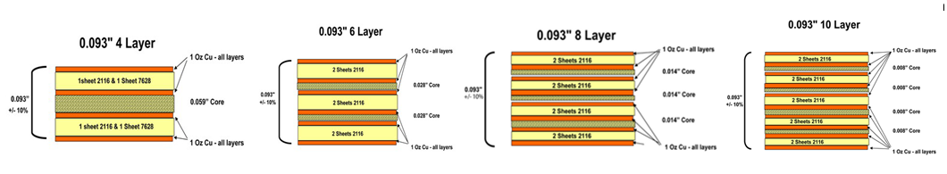
| Layer | 10 layers |
| Total Pins | 11,350 |
| Board thickness | 1.6MM |
| Material | FR4 tg 170 |
| Copper thickness | 1 OZ (35um) |
| Surface Finish | ENIG |
| Min via | 0.2mm (8 mil) |
| Min line width/spacing | 4 / 4 mil |
| Solder Mask | Green |
| Silk screen | White |
| Technology | all vias filled with solder mask |
| Design tool | Allegro |
| Design type | High speed, HDI |
Pandawill does not fit the factory to the design, but rather, to reduce unnecessary complexity and risk, we fit the right design to the right factory. This makes a huge difference in that Pandawill works to the strengths and capabilities of the factories.
This awareness is achieved through a detailed knowledge of our factory capabilities and a true understanding of their technology and performance on a monthly basis. This information is provided to our account management and customer service/support teams so that we can compare technical capability to design requirements right from the very start of the quoting process. This is an automated process, which provides alternatives with regard to price, as well as technical capability. Having the best possible options is a prerequisite for manufacturing the highest quality products.
PCB design type: High-Speed, Analog, Digital-analog Hybrid, High Density/Voltage/Power, RF, Backplane, ATE, Soft Board, Rigid-Flex Board, Aluminum Board, etc.
Design tools: Allegro, Pads, Mentor Expedition.
Schematic tools: CIS/ORCAD, Concept-HDL, Montor DxDesigner, Design Capture, etc.
● High Speed PCB Design
● 40G / 100G System Design
● Mixed Digital PCB Design
● SI/PI EMC Simulation Design
Design Capability
Max design layers 40 layers
Max pin count 60,000
Max connections 40,000
Minimum line width 3 mil
Minimum line spacing 3 mil
Minimum via 6 mil (3 mil laser drill)
Maximum pin spacing 0.44mm
Max power consumption/PCB 360W
HDI Build 1+n+1; 2+N+2, X+N+X, Any layer HDI in R&D
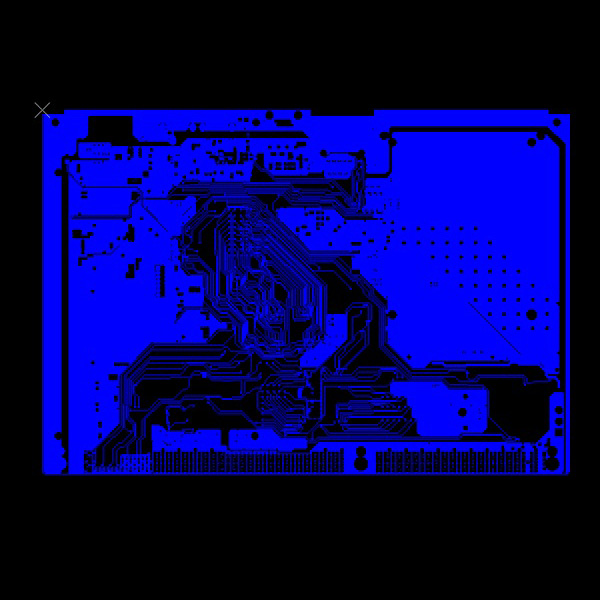
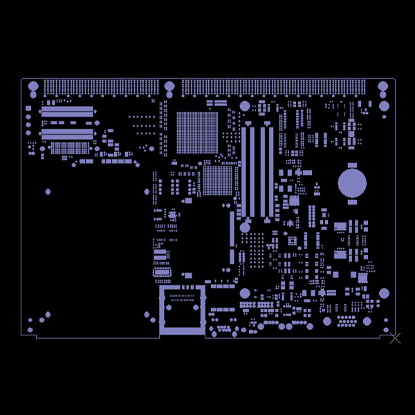
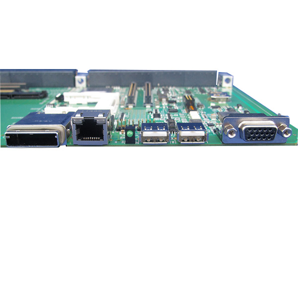
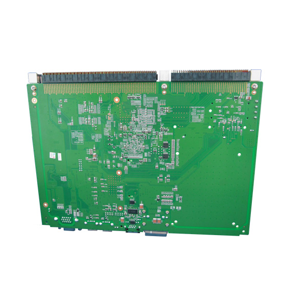
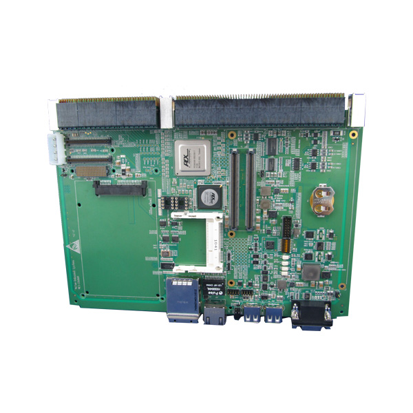
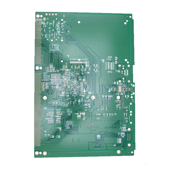
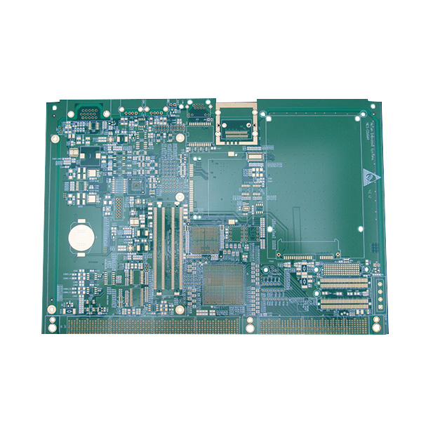
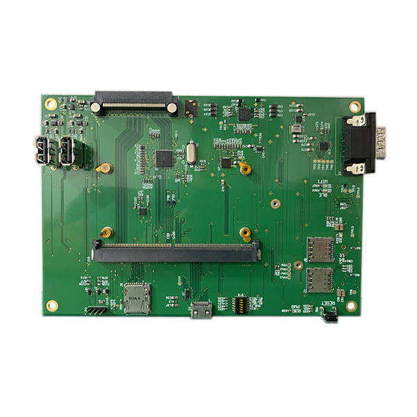
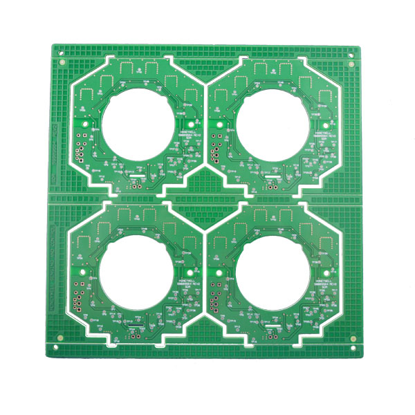
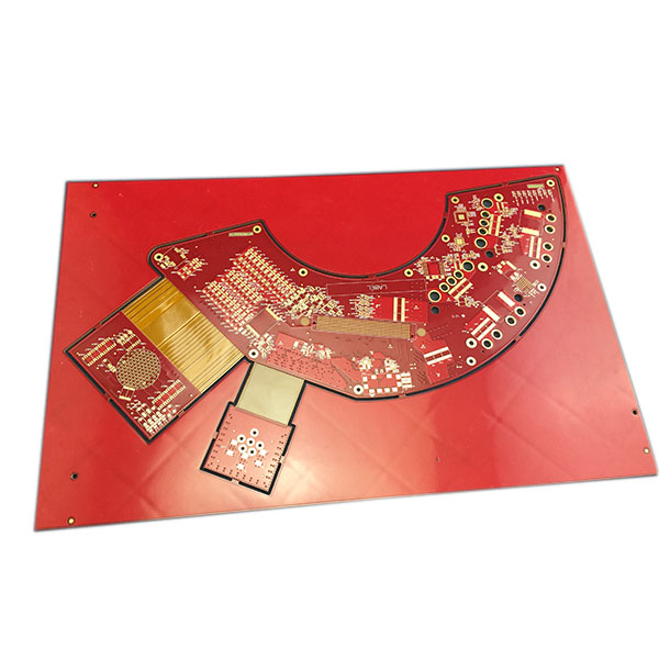
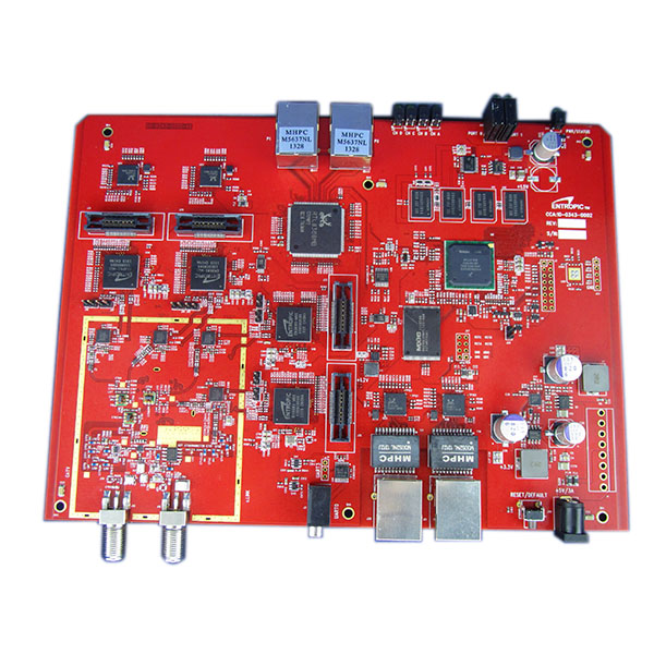
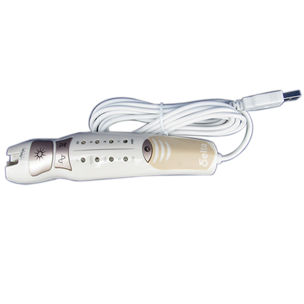
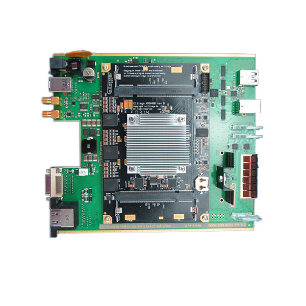
Product detail pictures:
Related Product Guide:
The corporation keeps to the operation concept "scientific management, superior quality and performance primacy, consumer supreme for Hot sale Pcb Design Engineer - 10 layer HDI PCB layout – Pandawill , The product will supply to all over the world, such as: Switzerland, US, Australia, Wide selection and fast delivery for you! Our philosophy: Good quality, great service, keep improving. We are looking forward that more and more oversea friends join in our family for further development near the future!
Factory equipment is advanced in the industry and the product is fine workmanship, moreover the price is very cheap, value for money!
Products categories
-
New Arrival China Prototype Pcb Fabrication - ...
-
Factory directly supply 6 Layer Pcb Manufacture...
-
Professional Design Bare Pcb Manufacturing - 1...
-
Reasonable price for 10 Layer Pcb Fabrication -...
-
High Quality Multi Layer Pcb Manufacturer - La...
-
Wholesale Price Aluminum Based Pcb Manufacturer...