100% Original Two Layer Pcb Design - RF PCB ceramic substrate + FR4 substrate – Pandawill
100% Original Two Layer Pcb Design - RF PCB ceramic substrate + FR4 substrate – Pandawill Detail:
Product Details
| Layers | 6 layers |
| Board thickness | 1.6MM |
| Material | IT-180A Tg170 + ceramic (280) |
| Copper thickness | 1 OZ(35um) |
| Surface Finish | (ENIG) Immersion gold |
| Min Hole(mm) | 0.203 plugged with solder mask |
| Min Line Width(mm) | 0.10mm (4 mil) |
| Min Line Space(mm) | 0.13mm (5 mil) |
| Solder Mask | Green |
| Legend Color | White |
| Impedance | Single Impedance & Differential Impedance |
| Packing | Anti-static bag |
| E-test | Flying probe or Fixture |
| Acceptance standard | IPC-A-600H Class 2 |
| Application | Telecom |
RF PCB
In order to meet increasing demands for Microwave & RF Printed Circuit Boards for our customers all around the world, we have increased our investment over the last few years so that we have become a world class manufacturer of PCBs using high frequency laminates.
These applications typically require laminates with specialized electrical, thermal, mechanical, or other performance characteristics that exceed those of traditional standard FR-4 materials. With our many years of experience with PTFE-based microwave laminate, we understand the high reliability and tight tolerance requirements of most applications.
PCB Material For RF PCB
Will all the different features of every RF PCB application, we have developed partnerships with the key material suppliers such as Rogers, Arlon, Nelco, and Taconic just to name a few. While many of the materials are very specialized, we do hold significant stock of product in our warehouse from Rogers (4003 & 4350 series) and Arlon. Not many companies are prepared to do that given the high cost of carrying inventory to be able to respond quickly.
High technology circuit boards fabricated with high frequency laminates can be difficult to design because of the sensitivity of the signals and the challenges with managing the thermal heat transfer in your application. The best high-frequency PCB materials have low thermal conductivity versus the standard FR-4 material used in standard PCBs.
RF and microwave signals are very sensitive to noise and have much tighter impedance tolerances than traditional digital circuit boards. By utilizing ground plans and using a generous bend radius on impedance controlled traces can help make the design perform in the most efficient manner.
Because wavelength of a circuit is frequency dependent and material dependent, PCB materials with higher dielectric constant (Dk) values can result in smaller PCBs as miniaturize circuit designs can be used for specific impedance and frequency ranges. Oftentimes high-Dk laminates (Dk of 6 or higher) are combined with lower cost FR-4 materials to create hybrid multilayer designs.
Understanding the coefficient of thermal expansion (CTE), dielectric constant, thermal coefficient, temperature coefficient of dielectric constant (TCDk), dissipation factor (Df) and even items like relative permittivity, and loss tangent of the PCB materials available will help the RF PCB designer create a robust design that will exceed the required expectations.
Wide Ranging Capabilities
In addition to standard Microwave/RF PCBs our capabilities using PTFE laminates also include:
Hybrid or Mixed Dielectric Boards (PTFE/FR-4 combinations)
Metal Backed and Metal Core PCBs
Cavity Boards (Mechanical and Laser Drilled)
Edge Plating
Constellations
Large Format PCBs
Blind/Buried and Laser Via’s
Soft Gold and ENEPIG Plating
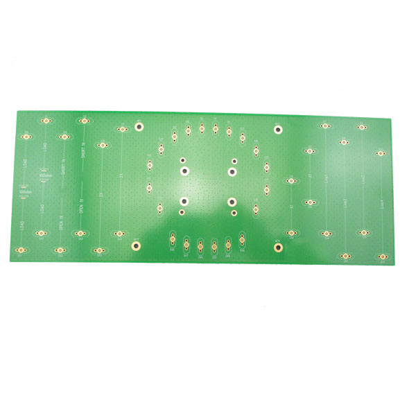
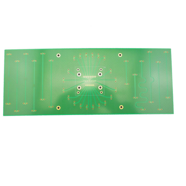
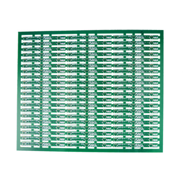
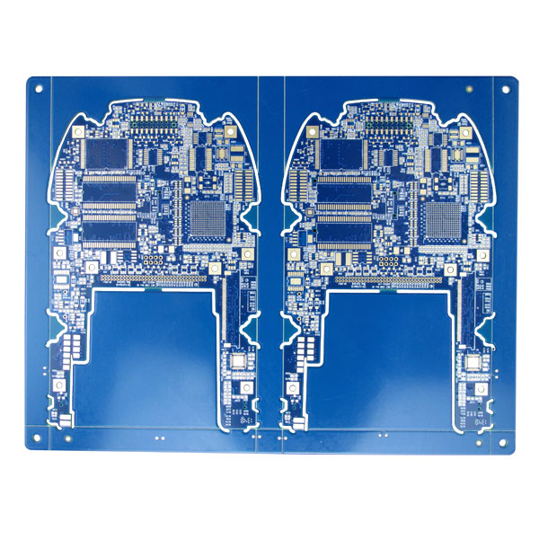
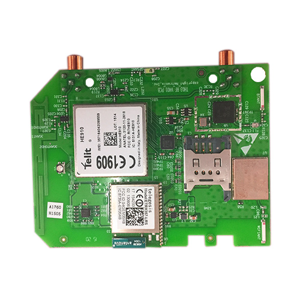
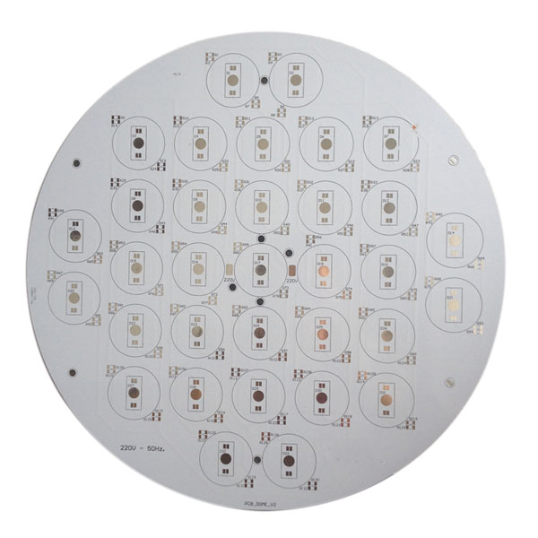
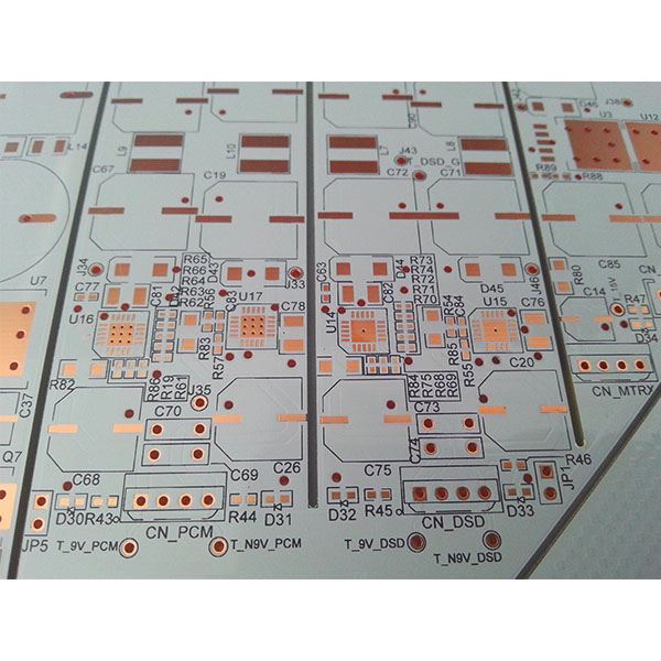
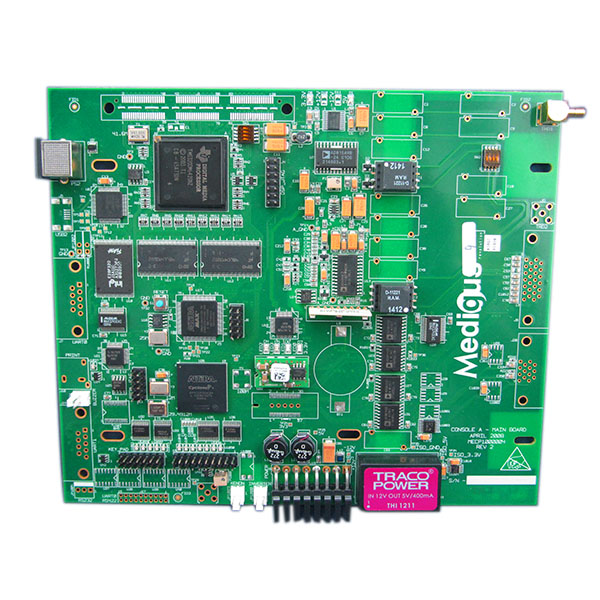
Product detail pictures:
Related Product Guide:
With reliable excellent approach, great name and ideal consumer services, the series of products and solutions produced by our company are exported to many countries and regions for 100% Original Two Layer Pcb Design - RF PCB ceramic substrate + FR4 substrate – Pandawill , The product will supply to all over the world, such as: Pretoria, Liverpool, Croatia, Look forward to the future, we'll focus more on the brand building and promotion . And in the process of our brand global strategic layout we welcome more and more partners join us, work together with us based on mutual benefit. Let's develop market by fully utilizing our in depth advantages and strive for building.
As an international trading company, we have numerous partners, but about your company, I just want to say, you are really good, wide range, good quality, reasonable prices, warm and thoughtful service, advanced technology and equipment and workers have professional training, feedback and product update is timely, in short, this is a very pleasant cooperation, and we look forward to the next cooperation!
Products categories
-
Super Purchasing for Polyimide Pcb Manufacture ...
-
Good Quality 20 Layer Pcb Manufacturer - 10 la...
-
Cheap PriceList for Kb Laminate Pcb Manufacture...
-
Factory Cheap 14 Layer Pcb Manufacturer - Alum...
-
Best Price on Smt Pcb Assembly - Metal core PC...
-
Big Discount Fr4 Pcb Manufacturer - Ultrasound...